Laser Control for Trapped-Ion Quantum Computing
Quantum computing is a rapidly evolving field that promises
exponential speedups for problems which are
intractable for classical computers.
One of the leading platforms for quantum computing is based on trapped ions,
which are charged atoms that have been trapped with
electric fields and are controlled with lasers.
Trapped ions offer high-fidelity quantum operations,
long coherence times, and potential for scalability.
However, trapped ions also pose significant challenges
for the control hardware that drives the quantum operations.
The control hardware needs to generate many channels
(one per trapped-ion qubit) with precise and flexible pulses
to manipulate the quantum states of the ions.
Recently there have been a number of advances in optical
technology that enable 10s of on-chip channels in
a compact form factor. However, the electronics to
control these channels at the requisite ~100MHz
resolution has lagged behind.
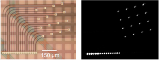
Thus we are developing a system that can provide control
for a recent photonic integrated chip with 16 optical channels,
as pictured below. Our electronic hardware is extensible
to be compatible with future device iterations with even more channels.
Source: 2210.03100.pdf (arxiv.org)
FPGA controller for trapped ion quantum device experiments
The project aims to build a device that can generate various
voltage signals with high precision using chips that can be
programmed and adjusted for different hardware purposes.
To achieve this goal, the project uses FPGAs,
which are ideal for pulse generators as they
enable reconfigurable, precise, and synchronous pulse generation
for various applications.
One such application is trapped ion quantum computing,
which requires precise control of laser pulses to
manipulate the quantum states of ions.
Our control hardware also features a high-speed
interface that can communicate with external data
converters and a CPU that can receive and translate commands from a PC.
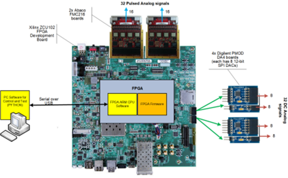
Overview of the FPGA systems, with all necessary peripherals included.
The DACs
The project involves the use of two different
types of digital-to-analog converters (DACs)
to generate analog signals from digital values.
The first is the Pmod DA4, a module that contains eight
DACs and communicates with the FPGA via a
serial peripheral interface (SPI).
We connect the Pmod to the FPGA using the
Pmod connectors on the FPGA board.
The second type of DAC is the Abaco FMC216,
a high-performance module that can produce signals
with a resolution of 16 bits and a data rate of
up to 1.25 Gbps per channel. The FMC216 communicates with the
FPGA using the JESD204B protocol,
a high-speed serial interface for data converters.
Interacting with the FPGA
The FPGA has a built-in ARM CPU that runs a
custom program that acts as an interface between the FPGA and a PC.
The program receives and translates these commands
into signals that control the modules in the FPGA.
The high-speed CPU buses provide the modules with
the desired pulse values and also configure the
timings of the pulse outputs.
Each module is equipped with a data transfer process
that allows the module to exchange data with the FPGA’s CPU data bus.
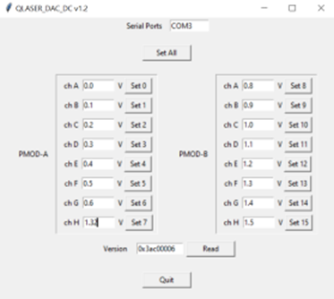
User Interface for setting the digital voltages
DC Control
There are two major parts to the hardware:
a static DC and an analog pulse control.
The DC control module is a key component of the FPGA-based
system that enables the regulation of the voltage levels of
up to 32 channels.
This module is suitable for applications that demand
fine-grained and static voltage regulation,
such as controlling the voltage levels of the electrodes
that confine and transport the trapped ions.
The module operates with the Pmod DAC board,
which outputs the desired voltage value.
It also allows the FPGA to communicate with the DAC board
via the SPI bus and handles the SPI bus protocol and timing.
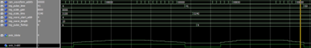
The functionality of the DC control module has been
verified in both simulation and hardware environments.
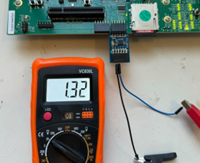
One of the channels set at static 1.32 V, with
a multimeter confirmed the voltage output.
Pulsed Control
The analog pulse module is a flexible and precise
system that uses the FPGA’s onboard memories to
store and generate various pulse shapes.
Each memory unit contains the data values of the pulse parameters,
such as shape, duration, and amplitude.
An integrated controller reads these values and
produces the desired signal shapes on the output channels.
The module has 32 output channels, each of which can produce
a programmable pulse shape with sub-microsecond reconfigurability.
The module also synchronizes the external DACs with
a high-resolution clock and sets the timing of each channel.
The module can store and execute multiple experiments on all
32 channels, triggered by an external signal, with a
resolution of 10 ns and a maximum duration of 50 ms.
Pulses are generated with two different time scales.
Waves generated via ModelSim
Collaboration
This project is a collaboration between the labs of
Prof. Sara Mouradian
and
Prof. Scott Hauck,
with substantial help from Geoff Jones.
Researchers: Eric Yu, Tyler Hsia