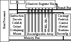
Figure 1. The overall Chimaera architecture.
Current mixed processor-FPGA systems suffer from a communication bottleneck between the processor and the reconfigurable logic. By placing the reconfigurable logic in a separate chip from the processor, the limited off-chip bandwidth and added delay interfere in efficient FPGA-processor communication. The resulting overhead requires that large chunks of the application code must be mapped to the reconfigurable logic to achieve any performance benefits at all. This means that relatively few applications can benefit from current adaptive systems, and they must be hand-mapped in order to achieve high enough performance benefits to justify the hardware costs and extra complexities. Also, huge reconfiguration times can overwhelm the benefits of reconfigurable logic, again limiting the types of applications that can benefit from reconfigurable logic. All of these factors keep adaptive computing from entering the mainstream, and drive up the cost and complexity of these systems.
We are developing a complete adaptive computing system, including both hardware resources and software mapping tools, which tightly integrates reconfigurable logic with standard processors. By removing the communication bottleneck, and by virtually eliminating the reconfiguration time overhead, we produce a system that can support general-purpose computing. Hand-mapped algorithms to such a system can expect a performance improvement of more than two orders of magnitude. We will also develop an efficient compilation system which can automatically generate mappings for the reconfigurable logic in time comparable to standard software compilation. By using such a system to automatically deliver a factor of 2-4 speedup for general purpose computing, and by providing standard libraries which can deliver an order of magnitude performance improvement for important classes of applications, we enable a new, mass-market computing paradigm. This will create a commercial adaptive computing system which can still provide several orders of magnitude performance improvement for hand-tuned applications, with COTS cost benefits.
The primary strength of a reconfigurable coprocessor (RCP) or functional unit (RFU) is the ability to customize the hardware to a specific program's requirements. Thus, when a communications program is active the reconfigurable logic might contain data compression and decompression routines, while when a rendering package is running the reconfigurable logic would be switched to support graphics operations. A more complex application, such as a complete word processor, might have different mappings to the reconfigurable logic for different sections of the code, with text search routines active in one phase of the code's operation, and postscript acceleration routines for another. While these operations may not provide as big a performance improvement as custom hardware due to the inevitable overheads inherent in reconfigurable logic, by being able to accelerate most or all applications running on a system they provide performance gains for a much larger class of problems.
In order to efficiently support these demands we are developing the Chimaera Reconfigurable Functional Unit. The Chimaera system treats the reconfigurable logic not as a fixed resource, but instead as a cache for RFU instructions. Those instructions that have recently been executed, or that we can otherwise predict might be needed soon, are kept in the reconfigurable logic. If another instruction is required, it is brought into the RFU, overwriting one or more of the currently loaded instructions. In this way, the system uses partial run-time reconfiguration techniques to manage the reconfigurable logic. This does require that the reconfigurable logic be somewhat symmetric, so that a given instruction can be placed into the RFU wherever there is available logic.
In order to use instructions in the RFU, the application code includes calls to the RFU, and the corresponding RFU mappings are contained in the instruction segment of that application. The RFU calls are made by special instructions which tell the processor to execute an RFU instruction. As part of this RFU call an instruction ID is specified which determines which specific instruction should be executed. If that instruction is present in the RFU, the result of that instruction is written to the destination register (also contained in the RFU call) during the instruction's writeback cycle. In this way, the RFU calls act just like any other instruction, fitting into the processor's standard execution pipeline. If the requested instruction is not currently loaded into the RFU, the host processor is stalled while the RFU fetches the instruction from memory and properly reconfigures itself. Note that this reconfiguration time can be quite significant. Thus, care must be taken to avoid constant reloading of the RFU.
Current RFU architectures (such as the PRISC system [Razdan94a, Razdan94b]) use a standard invocation model, where an instruction specifies the operations to perform, the operand source registers, and the destination register. This limits the complexity of the operations possible, and does not allow for concurrent operation of the RFU and the host processor. As part of this research we are developing a speculative execution model for computation, which promises greater performance and allows more complex functionality to be migrated to the reconfigurable logic. As shown in Figure 1, the reconfigurable logic could be given direct read access to a subset of the registers in the processor (either by adding read connections to the host's register file, or by creating a shadow register file which contains copies of those registers' values). An RFU configuration itself determines from which registers it reads its operands. A single RFU instruction can read from all of the registers connected to the RFU, allowing a single RFU instruction to use up to nine different operands. Thus, the RFU call consists of only the RFUOP opcode, indicating that an RFU instruction is being called, an ID operand specifying which instruction to call, and the destination register operand. Just as importantly, an RFU instruction currently loaded into the RFU does not have to wait for the occurrence of an RFU call in the instruction stream to begin executing, since it already knows which registers it needs to access. In fact, all loaded RFU instructions "speculatively" execute during every processor cycle, though their results are only written back to the register file when their corresponding RFU call is actually made. This means that an RFU instruction can in fact use multiple cycles to execute without stalling the host processor. For example, assume that RFU instruction #12 uses the values in register R0...R3, and these values are computed in the four previous cycles. The instruction stream for this situation might look like the following:
R0 = R8 - R9; R1 = R10 * 2; LOAD R2; LOAD R3; R16 = RFUOP #12;
In this example, while the RFU instruction might only have one cycle (its normal execute cycle) to use the value from register R3, it will have at least four cycles to use the value from R0, three cycles to use the value from R1, and two cycles to use the value from R2. As long as late-arriving operands are not needed until near the end of an RFU computation, much more complex operations can be done inside the RFU than are possible in a single clock cycle. Thus, with careful RFU mapping creation and register assignment very complicated computations can be performed.
The Chimaera architecture is shown in Figure 1. The main component of the system is the Reconfigurable Array, which consists of FPGA-like logic designed to support high-performance computations. It is here that all RFU instructions will actually be executed. This array gets its inputs directly from the host processor's register file, or a shadow register file which duplicates a subset of the values in the host's register file. Next to the array is a set of Content Addressable Memory locations, one per row in the Reconfigurable Array, which determine which of the loaded instructions are completed. The CAMs look at the next instruction in the instruction stream and determine if the instruction is an RFUOP, and if so whether it is currently loaded. If the value in the CAM matches the RFUOP ID, the value from that row in the Reconfigurable Array is written onto the result bus, and thus sent back to the register file. If the instruction corresponding to the RFUOP ID is not present, the Caching/Prefetch control logic stalls the processor, and loads the proper RFU instruction from memory into the Reconfigurable Array. The caching logic also determines which parts of the Reconfigurable Array are overwritten by the instruction being loaded, and attempts to retain those RFU instructions most likely to be needed in the near future. Reconfiguration is done on a per-row basis, with one or more rows making up a given RFU instruction.
Figure 1. The overall Chimaera architecture.
The Reconfigurable Array is shown in Figure 2 and Figure 3. This architecture has been inspired by the Triptych FPGA [Hauck92, Borriello95, Ebeling95], the Altera FLEX 8000 series [Altera95], and PRISC [Razdan94a, Razdan94b]. The routing structure is shown in Figure 2. The reconfigurable logic is broken into rows of logic cells between routing channels. Within that row, there is one cell per bit in the processor's memory word, so for a 32-bit processor there are 32 cells per row. All cells in a given column I have access to the Ith bit of registers R0-R8, allowing it to access any two of these bits. Thus, a cell in the rightmost (0th) column in the reconfigurable array can read any two least significant bits from registers R0 through R8. Which register(s) a cell accesses is determined by its configuration, and different cells within the array can choose which registers to access independently. We believe that such an architecture can efficiently support the demands of adaptive computing, and effectively implement the proposed speculative execution model. As part of this research, we are implementing and refining the Reconfigurable Array architecture described here, and demonstrating its effectiveness in supporting general-purpose adaptive computing.
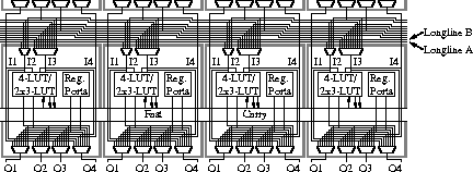
Figure 2. The Chimaera Reconfigurable Array routing structure.
The logic block for the Reconfigurable Array is shown in Figure 3. The logic block takes the four inputs to the cell and shuffles them (via muxes 1-4) into intermediate signals W, X, Y, and Z. The logic block itself can be configured as a 4-LUT, two 3-LUTs, or a 3-LUT and a carry computation. By using this carry configuration arithmetic and logical operations such as addition, subtraction, comparison, parity and others can be supported very efficiently. Note that Figure 3 represents the functionality possible in Chimaera's logic block, but not the actual implementation. We believe that higher-performance carry computations are possible, based upon high-performance adder design. Specifically, instead of relying on a simple ripple-carry scheme, carry schemes such as the Brent-Kung or Carry Select structures could be used to achieve an order of magnitude faster carry propagation. Our initial work on this concept is contained in [Hauck97]. We are developing VLSI implementations of these high-performance carry chain concepts. We are also developing a complete Reconfigurable Array implementation, including the proposed logic and routing structure, as well as the high-performance carry chains. When combined, we believe this architecture has the potential to deliver an extremely high-performance adaptive computing substrate.
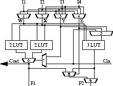
Figure 3. The Chimaera Reconfigurable Array logic block.
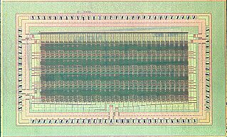
Figure 4. The Chimaera test chip. A fully-functional prototype of the array
developed in 1998.
 Scott Hauck
Matt Hosler
Tom Fry
Jeff Kao
Katherine Compton
Adaptive Computing
Multi-FPGA Systems & Rapid-Prototyping
Triptych/Montage FPGA Architectures
Scott Hauck
Matt Hosler
Tom Fry
Jeff Kao
Katherine Compton
Adaptive Computing
Multi-FPGA Systems & Rapid-Prototyping
Triptych/Montage FPGA Architectures
S. Hauck, M. M. Hosler, T. W. Fry, "High-Performance Carry Chains for FPGAs" (PDF), to appear in IEEE Transactions on VLSI Systems.
S. Hauck, Z. Li, E. J. Schwabe, "Configuration Compression for the Xilinx XC6200 FPGA" (PDF), IEEE Transactions on Computer-Aided Design of Integrated Circuits and Systems, Vol. 18, No. 8, pp. 1107-1113, August, 1999.
S. Hauck, M. M. Hosler, T. W. Fry, "High-Performance Carry Chains for FPGAs" (PDF), ACM/SIGDA International Symposium on Field-Programmable Gate Arrays, pp. 223-233, 1998.
S. Hauck, "Configuration Prefetch for Single Context Reconfigurable Coprocessors" (PDF), ACM/SIGDA International Symposium on Field-Programmable Gate Arrays, pp. 65-74, 1998.
S. Hauck, Z. Li, E. J. Schwabe, "Configuration Compression for the Xilinx XC6200 FPGA" (PDF), IEEE Symposium on FPGAs for Custom Computing Machines, pp. 138-146, 1998.
S. Hauck, "The Future of Reconfigurable Systems" (PDF), Keynote Address, 5th Canadian Conference on Field Programmable Devices, Montreal, June 1998.
Z. Li, S. Hauck, "Don't Care Discovery for FPGA Configuration Compression" (PDF), ACM/SIGDA International Symposium on Field-Programmable Gate Arrays , pp. 91-98, 1999.
S. Hauck, W. D. Wilson, "Abstract: Runlength Compression Techniques for FPGA Configurations" (PDF), IEEE Symposium on FPGAs for Custom Computing Machines, 1999.
K. Compton, S. Hauck, "Mapping Methods for the Chimaera Reconfigurable Functional Unit" (PDF), Northwestern University, Dept. of ECE Technical Report, 1997.
S. Hauck, W. D. Wilson, "Runlength Compression Techniques for FPGA Configurations" (PDF), 1999.
A. Ye, N. Shenoy, S. Hauck, A. Moshovos, P. Banerjee, "A C Compiler for a Processor with a Reconfigurable Functional Unit" (PDF), 1999.