Cell-Size Optical Microscope
In this
project, we plan to build a microscope, whose size is same as that of a cell.
This technology will be built on our recent work on low-contrast metasurface
optics, our expertise on electro-optic materials (2D materials, complex oxides
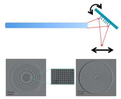
and phase change materials) and computational imaging. Figure 1 shows a typical
schematic of the proposed device. The microscope will be mounted on an optical
fiber. The optical element will be made of metasurface, which allows extremely
small focal-length lens with high numerical aperture, while preserving a
compact form-factor. This lens can be scanned to create an image. We will
explore MEMS based technology to scan the lens in the beginning. However, MEMS
technology will ultimately limit the overall size, and we will actively explore
electro-optic tuning of the optical elements, by integrating new materials on
the metasurface. Finally, the image gets distorted when it propagates through
the optical fiber. Using computational imaging techniques, we will circumvent
the distortions. Specifically, we will measure the transmission matrix of the fiber,
and multiply the captured image with the inverse of the transmission matrix.

Figure 1:
Typical schematic of the microscope. The light will be carried by an optical
fiber. The optical element can be a simple lens, or more complicated optical
elements (which can be used to control phase, polarization and frequency of
light). The optical element needs to be scanned to capture an image from the
tissue. For scanning we are pursuing MEMS based technology, as well as electro-optic
technologies which do not require any moving parts.
However,
the versatility of the metasurface, can be realized by
building optical elements, that can simultaneously control, phase, polarization
and frequency of light. Further, metasurfaces can truly enable freeform optics,
where multiple optical elements are combined to create one optical surface,
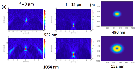
which is difficult to create by conventional optical manufacturing. Figure 2
shows some of the simulated result of unusual optical elements, that
metasurface can be used to build.

Figure 2: (a) Simulated performance of a lens, which focuses at the same
spot for 532nm and 1064nm (needed for two photon microscopy); (b) Different
mode profiles for different wavelengths in the focal plane, which is needed for
the STED type super-resolution microscopy.