for next-generation signal processing algorithms
|
FPGA-based cochlear implant controller for next-generation signal processing algorithms |
The goal of this project is to develop an interface board between the existing Cochlear Implants and the smartphones, allowing new signal processing algorithms to be tested and implemented on the smartphones.
A cochlear implant is a surgically implanted device that helps to produce useful hearing sensations to a person who is profoundly deaf or severely hard-of-hearing due to sensorineural hearing loss, caused by damage to tiny hair cells in the part of the inner ear called the cochlea. Unlike the hearing aids, which just amplify sound, cochlear implant substitute for the damaged part of the ear to provide sound signals to the brain. The device provides direct electrical stimulation to the auditory (hearing) nerve in the inner ear by bypassing the damaged hair cells.
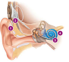
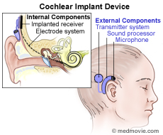
Figure 1. Components of cochlear implant. (http://www.hearinghouse.co.nz/children-families/appropriate-amplification/)
(http://www.fda.gov/MedicalDevices/ProductsandMedicalProcedures/ImplantsandProsthetics/CochlearImplants/)
Cochlear implants have external components (behind the ear) and internal components (surgically implanted) that work together to allow the user to perceive the sound. The external components include a microphone, a body-worn or a Behind-The-Ear (BTE) speech processor and a RF transmitter. The microphone captures sound, allowing BTE speech processor (1) to convert it into digital signals. These digitally coded sound signals are transmitted (2) across the skin via radio waves using the RF transmitter. The internal components include a RF receiver and electrodes. The receiver (3) converts the digitally-coded sound signals into electrical impulses and sends them along the electrode array (placed in cochlea). The electrodes (4) stimulate the auditory nerve fibres to send information to the brain.
We propose a portable mechanism for prototyping new processing algorithms by coupling the existing implants with the smartphones. The coupling is handled by a newly developed interface board which not only allows the interaction between the implants and the smartphones, but also ensures that it is safe for the users. The idea is to replace the currently used body-worn or BTE processor with the FPGA-interface board and the smartphone. Most of the computation on the interface board is done with FPGAs.
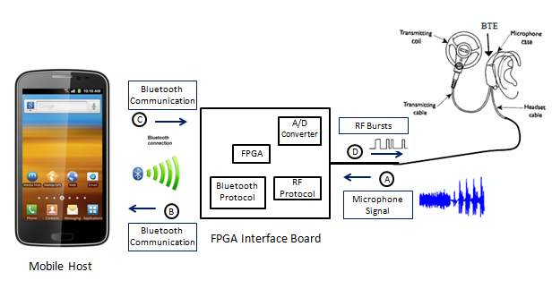
Figure 2. Overview of the system, communication between the smartphone and the implant, using the FPGA interface board.
The interface board handles the communication from the microphone in each BTE of the implant to the smartphone, and from the smartphone back to the transmitter of the implant. The acoustic signal (A) is picked up by the microphone located in the BTE (Behind-The-Ear). These signals (one or two, depending on the number of implants the patient has) are sent to the interface board. The FPGA's built in ADCs will sample the signal to provide digital values. This sampled signal is (B) then sent to the smartphone for processing. Currently, we plan to use Bluetooth to communicate between the phone and the interface board (as it eliminates some cabling), but a USB-wired protocol can also be used. Once the data has been processed by the phone, it produces a set of amplitudes representing the energy levels of each electrode. This set is transmitted (C) back to the interface board. The FPGA will perform the safety and integrity check on the data coming from the smartphone, to ensure that only FDA approved stimulation parameters are transmitted to the implant. The interface board will prepare the verified data for transmission to the RF transmitter of the cochlear implant, via the cable, (D) in form of RF bursts, with 5MHz carrier frequency. Note that this processing must enforce all the safety requirements for this communication and also meet the communication protocol requirement for the cochlear implant used.
The external unit of cochlear implant needs to provide not only reliable communication protocols including a signal modulation method, bit coding, frame coding and synchronization, but also high efficiency power amplifier and immunity to electromagnetic interference (EMI). The information that is received from the mobile phone is a stream of digital data. This information is fed through a DAC (digital-to-analog converter) to convert it into an analog signal. Next, the signal is modulated to a carrier frequency of 5MHz, using amplitude shift keying (ASK) modulation technique for RF transmission. 1 is coded with ON cycles of 5MHz, i.e. RF burst is present for those cycles, and 0 is coded with OFF cycles of 5MHz, i.e. RF burst is not present for those cycles. The next operation is to filter the signal, restricting the signal to a selected bandwidth, and attenuating any out-of-band noise or any high-frequency signal. The RF link uses frame or packet coding schemes to transmit specific stimulus parameters such as, pulse amplitude, pulse duration, pulse gap, active electrode and return electrode and the stimulation mode. Frame coding schemes can be classified by either the embedded mode (embedded protocol) or expanded mode (expanded protocol) depending on the cochlear implant. Next, the signal goes through the RF power amplifier, which provides the final boost to the RF bursts. We are planning to provide all these functionalities on the FPGA interface board, but if a cochlear implant company has some other additional specifications, they can be implemented either by reprogramming the FPGA board or by adding a daughter board equipped with that function.
For initial prototyping, we are using Odyssey MAX 10 FPGA evaluation kit, which includes Altera MAX 10 FPGA and Odyssey Bluetooth SMART Sensor board to provide USB and wireless communication protocols. MAX 10 devices are low-cost, low-power devices, which enables longer battery life, reducing the amount of recharging required. These are non-volatile programmable logic devices with integrated Analog-to-Digital Converters(ADC's) and single-on-die flash memory, which enables them to retain the data even when they are turned-off, resulting in simple and fast configuration. The MAX10 ADC is a 1MHz successive approximation register (SAR) ADC. The final board will also have Digital-to-Analog Converters (DAC's) and RF protocol for sending the signals from the board to the RF transmitter and some other support elements.