| Model Description
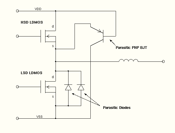
Neither the Standard Gummel-Poon nor the new VBIC95 BJT models are suitable for application to the parasitic bipolar effects in a LDMOSFET or LDMOS device. These standard models omit the reverse graded base structure (doping at the collector is higher than at the base) and the effects of the widely changing base width due to collector-base voltage changes. To our knowledge this is the only BJT model specifically designed for the parasitic BJT effects in LDMOS devices. The LDMOS, a smart power IC device, is usually implemented in pairs. The High-Side-Driver HST and the Low-Side-Driver LST are connected as shown in the Schematic. The HST has a parasitic PNP BJT and the LST has two parallel parasitic diodes that are here implemented in one diode model. Both the BJT and diode models are to be electrically connected to a pair of LDMOS models during simulation. These models are relatively simple so as not to significantly low the simulation speed of the LDMOS models . The diode model is identical with the diode model separately listed as an Intermediate Diode with Reverse Recovery |
||
| Schematic
|
||
| Model Parameters
and Default Values |
va = 350,
Qe = 1.92e-15, Qb2 = 3.84e-16, Qb3 = 5.76e-15, Qc = 3.84e-16, Qi = 1.33e-17, Tbase = 2.274e-8, Taub = 3e-5, Taue = 1e-7, Tauc = 1e-7, |
Early voltage
Emitter charge Base charge @ Node 2 Base charge @ Node 3 Collector charge Intrinsic charge Zero-bias Transit time Base region lifetime Emitter region lifetime Collector region lifetime |
| Model Parameters
and Default Values |
Model parameters are the same as those of the standard SPICE diode model with the addition of carrier lifetime "Tau" and the voltage "PhiB" needed to deplete the internal lightly doped region by one diffusion length. The standard SPICE diode includes only a diffusion transit time parameter "TT". Both "TT" and "Tau" are required for reverse recovery. Typically, "PhiB" is of similar magnitude as the junction breakdown voltage. | |
| Performance Level: | INTERMEDIATE | |
| Quality Classification: | 1B
Only limited testing has been performed. Model parameters are similar to those used in the discrete power BJT model. For use in VLSI design applications, they can be easily converted into a new parameter set based on device structure and process information. |
|
| Original Support for Model Development | CDADIC, 1997-98 | |
| Documentation | The parasitic BJT and diode models are described in the MSEE Thesis of Yafe Bi, "Compact Modeling of Power Bipolar Transistor and Parasitic Bipolar Transistor in LDMOS Structures", MSEE Thesis, University of Washington, December 1998 | |
| Download Model Source Code | BJT
parasitic Model (bjt)
Diode Model(diode) |
|