
Abstract
The development of ultra-compact integrated nanophotonic structures for communications, sensing, and signal processing has been of great interest lately. Recent progress in the development of miniaturized high-Q microresonators has resulted in orders of magnitude reduction in the size of functional integrated photonic structures. The possibility of low-power tuning of the resonance features in these structures has made the formation of reconfigurable photonic structures possible.
Among existing CMOS-compatible substrates, silicon (Si) and silicon nitride (SiN) have been used the most. Despite impressing progress in Si-based and SiN-based integrated photonics, neither substrate alone can be used for practical applications. Si (despite its good reconfigurability) suffers from strong nonlinear effects (especially at high light intensities) and relatively large free-carrier loss while SiN (with one order of magnitude lower loss and lower nonlinearity compared to Si) is very hard to tune. Thus, a reliable material system that combines ultra-loss-loss and high power handling with efficient and fast reconfigurability is of high demand in integrated nanophotonics.
In this talk, the recent achievements in the development and optimization of hybrid multi-layer CMOS-compatible material systems (e.g., SiN/Si, multi-layer Si/SiO2, etc.) to address all the practical requirements of ultra-fast and ultra-compact integrated photonic structures will be discussed. Using these hybrid material systems, a series of ultra-compact and high-performance reconfigurable photonic devices and subsystems that are formed by using high Q resonators will be demonstrated. The use of these devices and subsystems for realization of densely-integrated reconfigurable photonic chips for signal processing and sensing applications will be discussed.
Biography
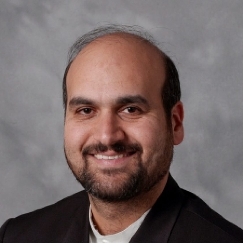
Ali Adibi is the director of Bio and Environmental Sensing Technologies (BEST) and a professor and Joseph M. Pettit chair in the School of Electrical and Computer Engineering, Georgia Institute of Technology.
His research group has pioneered several structures in the field of integrated nanophotonics for both information processing and sensing. He is the author of more than 140 journal papers and 400 conference papers. He is the editor-in-chief of the Journal of Nanophotonics, and the nanophotonic program track chair of the Photonics West meeting. He is the recipient of several awards including Presidential Early Career Award for Scientists and Engineers, Packard Fellowship, NSF CAREER Award, and the SPIE Technology Achievement Award. He is also a fellow of OSA, SPIE, and AAAS.